The single-transistor SMPS circuit board is popular for its small size, affordability, and simplicity. It's commonly found inside Chinese chargers for charging keypad mobile phone batteries.
These chargers are basic and inexpensive, employing a simple SMPS design. However, they are prone to damage. They operate with input voltages ranging from 110 to 220 volts at 47 to 63 Hertz, providing an output power of 5 volts at 800 milliamps.
Single Transistor Mobile Phone Charger Circuit Diagram
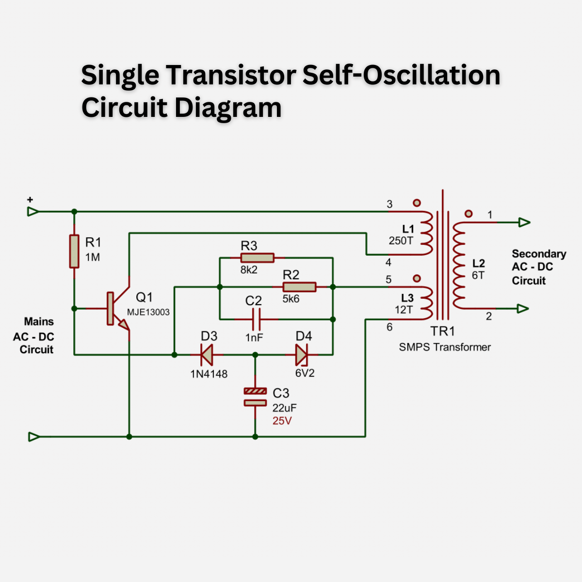
The schematic of a single transistor 5V 800mA mobile phone charger circuit is shown below.

Working Principle of Single Transistor Mobile Phone Charger Circuit
The single transistor switched mode power supply circuit works in three steps – Mains AC to DC conversion, Self-Oscillation, and Secondary AC to DC conversion.
Mains AC to DC Converter Circuit

When the input mains AC voltage passes through the diodes (D1 & D2), undergoing half-wave rectification, which converts it into DC voltage. This voltage is then smoothed using a capacitor (C1).
Single Transistor Self-Oscillation Circuit

Now, the DC voltage biases the MJE13003 transistor (Q1) through a base resistor (R1) and turns it on. This allows current to flow through the primary winding (L1) of the SMPS transformer (TR1). After a few milliseconds, the primary winding reaches its maximum inductance capacity.
Simultaneously, a low voltage begins to rise across the auxiliary feedback winding (L3) of the transformer. This voltage charges the capacitor (C2) negatively, with more power than the current flowing through the resistor (R2).
The negative voltage continues to flow to the base-emitter junction of transistor (Q1). As a result, the transistor turns off, interrupting the current flow through the primary winding. In addition, the negative voltage also flows through diode (D3) and charges the capacitor (C3).
At this moment, capacitor (C2) starts to discharge through its parallel resistors (R2 & R3). Meanwhile, the stored negative voltage in capacitor (C3) exceeds 6.2V, causing the Zener diode (D4) to become forward-biased. This helps discharge the excess voltage through the feedback winding (L3).
However, capacitor (C3) attempts to charge again, causing some negative voltage to be pulled down from the base-emitter of transistor (Q1). This results in base current flowing through resistor (R1) to bias the base of transistor (Q1) and restart the current flow through the primary winding (L1).
Therefore, the self-oscillation process repeats rapidly, typically at a frequency of around 22-50kHz, depending on various parameters.
Secondary AC to DC Converter Circuit

Consequently, a step-down AC voltage is generated in the secondary winding (L2) with the same frequency. This secondary voltage is then rectified (half-wave) using a single Schottky diode (D5) and smoothed by a capacitor (C4).
The output voltage can initially reach as high as 8-9 volts under no load but quickly drops to 5V when a load is connected. A 3mm red LED (D6) with a current-limiting resistor (R4) is connected in parallel at the output to indicate the output status.
SMPS Transformer Details
| Model | 50Hz SE-EE-25X9X6. |
| Phase | Single. |
| Usage | SMPS only. |
| Core Type | Small EE-type ferrite core transformer with air gap. |
| Primary Winding (L1) | 250 turns with 36 to 40 SWG insulated copper wire. |
| Secondary Winding (L2) | 6 turns of 26 to 28 SWG insulated copper wire. |
| Feedback Winding (L3) | 12 turns with 36 to 40 SWG insulated copper wire. |


Thank you Sir
ReplyDeleteSir ..Jou are amazing best explanation I found ..Have u any youtube channel
DeleteWhen your website or blog goes live for the first time, it is exciting. That is until you realize no one but you and your.
ReplyDeletehigh voltage rectifier diodes
Sir thanks for your diagram, i just want to know the name of transformer i can't find the transformer online bcz i don't know the name of transformer so kindly tell me the name?
ReplyDeleteHi Rana,
DeleteThe transformer model is 'EE16'.
You will not find this single phase SMPS transformer exactly the same online.
Therefore, you can make this transformer.
I have given the information about the transformer windings in this article.
Thanks SUBHAJIT
DeleteThanks Sir, can have possible to provide Transformer winding inductance and about required gap like Air gap or Zero gap or etc.
DeleteA small correction. You have not explained the function of the 1N5237 zener diode. This is very important, and its purpose is to limit the output voltage.
ReplyDeleteThanks for that information :)
Deletecould somebody tell which is D2, C2 and C3? The last was a great explanation.
ReplyDeleteSingle transistor mobile phone charger is a portable smps design with single transistor 13001.
ReplyDeletedscvdvx
ReplyDelete